Last updated on August 24th, 2023 at 02:26 pm
Digital Logic Circuit Notes
If you want to prepare for your university exams along with the GATE exam, you are at the right place!
The following Digital Logic Circuit Notes on the subject of Computer Organisation and Architecture will surely help you to achieve grace marks.
Along with these notes, you will find much more content and material while browsing Computer Organisation and Architecture and other subjects.
Digital Computer
- A binary digit is called a bit.
- Information is represented in digital computers in groups of bits.
- A computer system is subdivided into Hardware and Software
- The computer’s hardware consists of all the electronic components and electromechanical devices that comprise the physical entity of the device.
- Computer software consists of the instructions and data that the computer manipulates to perform various data-processing tasks.
- A sequence of instructions for the computer is called a program.
- The programs included in a systems software package are referred to as the operating system.
- The hardware of the computer is usually divided into three major parts :
- Central Processing Unit (CPU)
- Random Access Memory (RAM)
- Input-Output Processor (IOP)

Difference between Computer Organisation and Computer Architecture
| Computer Organisation | Computer Architecture |
|---|---|
| Concerned with the hardware design of the computer | Concerned with the functional behavior of the computer |
| Describes how things are done | Describes what has to be done |
| Deals with low-level designs | Deals with high-level designs |
| The implementation of the architecture is called the organization | As a programmer, you can view architecture as a series of instructions, addressing modes, and registers |
| Consists of physical units like circuit designs, peripherals, and adders | Comprises logical functions such as instruction sets, registers, data types, and addressing modes |
Logic Gates
- Binary information is represented in digital computers by physical quantities called signals.
- The two states represent a binary variable that can be equal to 1 or 0.
- For example, a particular digital computer may employ a signal of 3 volts to represent binary 1 and 0.5 volts to represent binary 0.
- The manipulation of binary information is done by logic circuits called gates.
- Each gate has a distinct graphic symbol and its operation can be described by means of an algebraic expression.
- The input-output relationship of the binary variables for each gate can be represented in tabular form by a truth table.
Also Read: Digital Component Notes
AND Gate
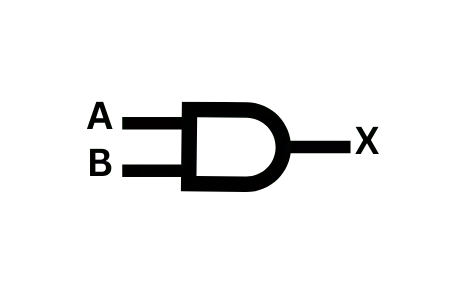
Algebraic function – x = A x B

OR Gate

Algebraic function – x = A + B

NAND Gate

Algebraic function – x = (A x B)’

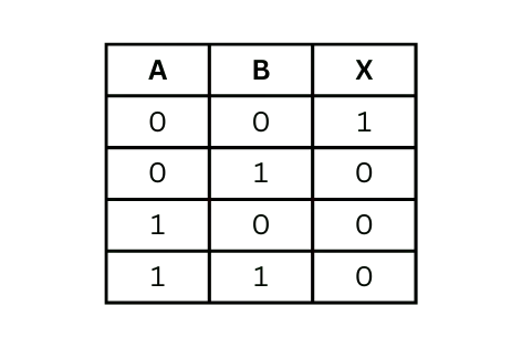
NOR Gate
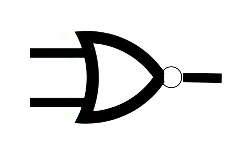
Algebraic function – x = (A + B)’
Buffer Gate

Algebraic function – x = A

NOT Gate

Algebraic function – x = A’

XOR Gate

Algebraic function – x = A ⊕ B or A’B + B’A

XNOR Gate

Algebraic function – x = (A ⊕ B)’ or A’B’ + AB

Boolean Algebra
- Boolean algebra is an algebra that deals with binary variables and logic operations.
- For a given value of the variables, the Boolean function can be either 1 or 0.
- Ex – F = x + y’z
Basic identities: –
| x + 0 = x | x.0 = 0 |
| x + 1 = x | x.1 = x |
| x + x =x | x.x = x |
| x + x’ =1 | x.x’ = 0 |
| x + y = y + x | x.y = y.x |
| x + ( y + z ) = ( x + y ) + z | x ( y.z ) = ( x.y ) z |
| x ( y + z ) = x.y + x.z | x + y.z = ( x + y ).( x + z ) |
| ( x + y ) ‘ = x’.y ‘ | ( x.y )’ = x’ + y’ |
| ( x’ ) ‘ = x | x + x.y = x |
De-Morgan’s Law:-
- ( x.y )’ = x’ + y’
- ( x + y )’ = x’.y’
Canonical and Standard Form
- Canonical Form – Boolean function can be expressed as Canonical Disjunctive Normal Form known as minterm and some are expressed as Canonical Conjunctive Normal Form known as maxterm
- In Minterm, we look for the functions where the output results in “1”
- Maxterm we look for a function where the output results in “0”.
- We perform the Sum of minterm also known as the Sum of products (SOP).
We perform Product of Maxterm also known as Product of sum (POS).
| x | y | z | Minterms (SOP) | Maxterms (POS) |
|---|---|---|---|---|
| 0 | 0 | 0 | m0 = x’.y’.z’ = min(x’,y’,z’) | M0 = x + y +z = max(x,y,z) |
| 0 | 0 | 1 | m1 = x’.y’.z = min(x’,y’,z) | M1 = x + y +z’ = max(x,y,z’) |
| 0 | 1 | 0 | m2 = x’.y.z’ = min(x’.y.z’) | M2 = x + y’ + z = max(x,y’,z) |
| 0 | 1 | 1 | m3 = x’.y.z = min(x’.y.z) | M3 = x + y’ + z’ = max(x,y’,z’) |
| 1 | 0 | 0 | m4 = x.y’.z’ = min(x,y’,z’) | M4 = x’ + y + z = max(x’,y,z) |
| 1 | 0 | 1 | m5 = x.y’.z = min(x,y’,z) | M5 = x’ + y + z’ = max(x’,y,z’) |
| 1 | 1 | 0 | m6 = x.y.z’ = min(x,y,z’) | M6 = x ‘+ y’ + z = max(x’,y’,z) |
| 1 | 1 | 1 | m7 = x.y.z = min(x,y,z) | M7 = x’ + y’ + z’ = max(x’,y’,z’) |
Combinational Circuit
- A combinational circuit is a connected arrangement of logic gates with a set of inputs and outputs.
- The n binary input variables come from an external source, the m binary output variables go to an external destination, and in between there is an interconnection of logic gates.
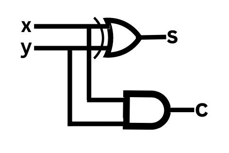
Half Adder
- A combinational circuit that performs the addition of two bits
- The input variables of a half-adder are called the augend and added bits
- The output variables are the sum (S) and carry (C)
- The sum represents the least significant bit
- Example – 1 + 1 = 10. Here S = 0 and C = 1
- S = x’.y + x.y’ = x ⊕ y
- c = x.y


Full Adder
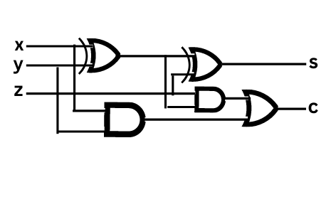
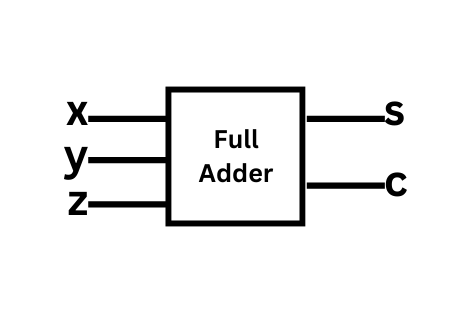
- A combinational circuit that forms the arithmetic sum of three input bits.
- It consists of three inputs and two outputs.
- Two of the input variables, denoted by x and y, represent the two significant bits to be added. The third input, z, represents the previous lower significant position carry.
- Two half-adders are needed to implement a full adder.

Final Words
From the above article, you must have gained knowledge about Digital Logic circuits. We hope that with the help of these notes you will be successful.
Also Read: Digital Component Notes